RF Circulator & Isolator: What to Watch Out For
Updated on:
Keywords: RF isolator,RF circulator,microwave isolator
This page focuses on how to deploy an RF isolator and an RF circulator correctly across bands and packages without altering system intent.
Introduction
When the engineering team is implementing RF circulators and RF isolators, the most common problem they encounter is not whether the devices are good or not, but whether they are used under the correct conditions and methods. Deviation from the bandwidth causes isolation to drop, excessive VSWR induces instability in the power amplifier, and underestimation of thermal coupling leads to long-term drift... All these directly affect the MTBF and maintainability. This article proceeds along two lines: "Precautions" and "Practical Guidelines", providing both hard and fast rules on the indicator side and executable steps from selection to maintenance, helping you to safely and stably utilize these two types of devices throughout their entire life cycle.
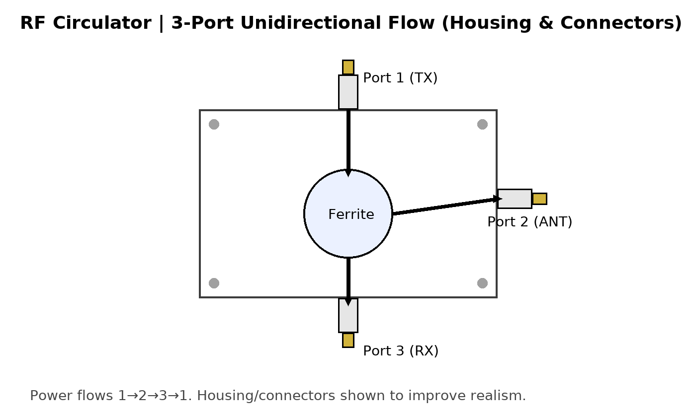
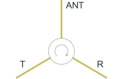
Diagram — RF circulator (housing & connectors).
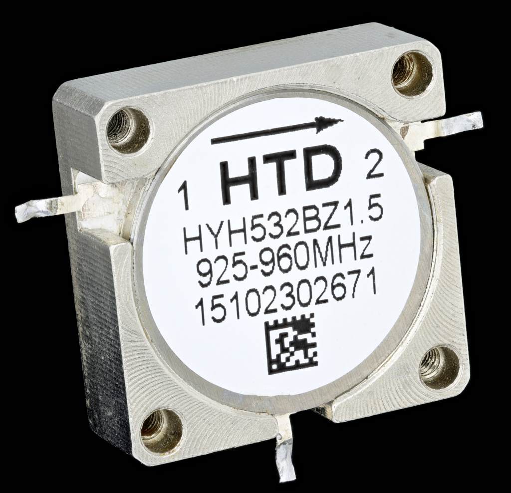
Photo — HYH532BZ1.5 RF circulator/isolator (coaxial). Source: Wikimedia Commons; Author: Mister rf; License: CC BY‑SA 4.0.
Usage Notes for RF Isolators and Circulators
1)Band & Bandwidth Matching
Most devices are narrowband. Start with BW_sel ≈ BW_sys × 1.1–1.2. During prototyping, sweep S‑parameters across the full temperature range (e.g., −40 to +85 °C) and verify edge‑of‑band isolation and group delay stability. A microwave isolator used near band edges will exhibit stronger drift, so margin matters.
2)Isolation vs Insertion Loss (IL)
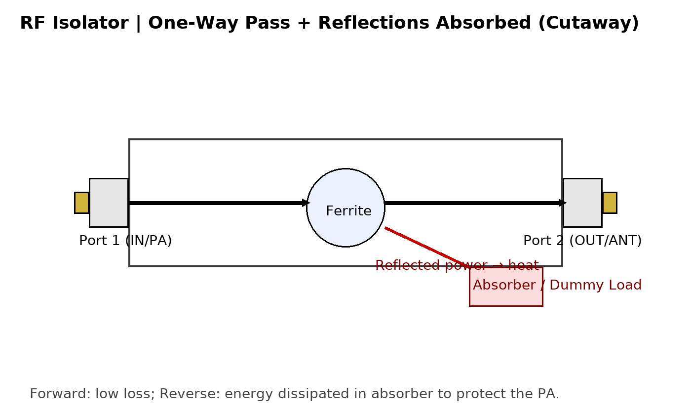
Diagram — RF isolator cutaway: reflected power absorbed → heat.
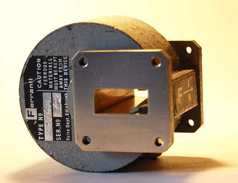
Photo — WG16 waveguide isolator (resonant absorption). Source: Wikimedia Commons; Author: Catslash; License: Public Domain.
Baseline goals: IL ≤ 0.3–0.5 dB; Isolation ≥ 20–25 dB. At higher bands and wider bandwidths, manufacturing tolerance and temperature drift hit hardest at the band edges. Track IL and isolation together, and avoid operating exactly at the limit for long durations.
3)Power Handling & Thermal Path
Specify peak envelope power, average power, and duty cycle. Estimate case temperature under worst cooling and derate accordingly. Ferrite magnetization shifts with heat; expect slow IL/isolation drift. Burn‑in should combine steady‑state load with thermal‑shock cycling.
4)VSWR Discipline & Return Loss Targets
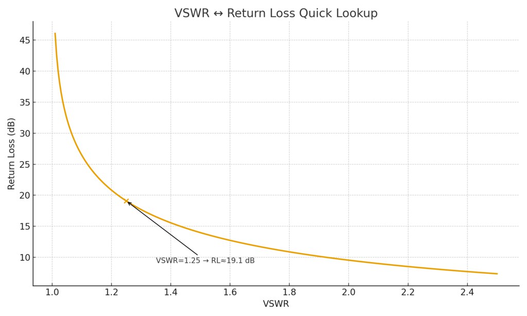
Diagram — VSWR ↔ Return Loss quick lookup.
Target VSWR ≤ 1.25:1 (return loss ≥ 19.1 dB). Antenna mismatch, array scanning, and temperature can change port impedances; plan for worst attitudes. Add limiters or over‑power protection to prevent PA stress and IMD spikes.
5)Package & Installation
| Package | Pros | Use Cases | Installation Notes |
|---|---|---|---|
| Microstrip | Compact, easy to integrate | Mid/low power | Consistent DK/thickness; via fences; impedance continuity |
| Drop‑in | Good shielding, serviceable | T/R modules | Diagonal torque steps; follow torque chart; avoid cavity strain |
| Coax | Wideband, test‑friendly | Lab/line/integration | Minimize adapters; keep bend radius; maintain shielding |
| Waveguide | High power, low loss | Radar/sat links | Flange flatness/seal; torque per standard |
6)EMC & Reliability
Strong magnetic fields (e.g., MRI 1.5/3 T) can bias ferrites. For space, consider radiation, vacuum heat paths, thermal cycles, and vib/shock. Prefer qualified or flight‑proven parts; perform TID/SEE assessments and monitor Temperature ↔ IL/Isolation/VSWR over life.
5‑Step Playbook
1)Selection
- BW_sel ≈ BW_sys × (1.1–1.2); define sub‑bands and margin.
- List PEP / average / duty; compute worst‑case thermal path and case temperature.
- Package vs power: microstrip/drop‑in for compact modules; coax/waveguide for high power.
- Environment: temperature range, vibration/shock, radiation, and vacuum cooling if applicable.
2)Isolation
- Low‑impedance ground; via fences; minimize gaps and discontinuities.
- Torque in diagonal steps as per vendor chart; avoid local stress.
- Impedance‑continuous routing; avoid sharp bends; minimize adapters.
3)Test (VNA + Thermal)
- Calibrate first (SOLT/TRL), then measure S‑parameters across the full band.
- Record IL/Isolation/VSWR over temperature and duty cycle.
- Thermal: exercise extremes and poor‑cooling cases; build temperature‑to‑spec curves.
- SPC: track mean/variance for lot consistency.
4)Operation
- Do not camp at spec limits; set alarms for power, temperature, and VSWR.
- Monitor VSWR and temperatures online; enable fast fault localization.
- Derate under hot ambient or heavy duty cycle.
5)Maintenance
- Periodic re‑test of S‑parameters and temperature drift.
- ESS: temperature cycling, vibration, and thermal shock for early‑life failures.
- Keep matched‑lot spares for critical chains.
Incoming QA Template (AQL + S‑parameters)
| Item | Sampling | Method/Threshold | Decision |
|---|---|---|---|
| Band/BW | AQL | VNA sweep; coverage ≥ 100% of target BW | Pass/Fail |
| Insertion Loss | Key points | IL ≤ 0.3–0.5 dB (per P/N) | Pass/Fail |
| Isolation | Key points | Isolation ≥ 20–25 dB | Pass/Fail |
| SWR | Key points | SWR ≤ 1.25:1 (RL ≥ 19.1 dB) | Pass/Fail |
| Consistency | SPC | Mean/variance within control limits | Pass/Fail |
| Thermal | SPC | Steady‑state load; ΔT < spec limit | Sample |
Quick Formulas
| Topic | Formula | Example |
|---|---|---|
| Return loss | RL = −20·log10|Γ|; |Γ| = (SWR−1)/(SWR+1) | SWR=1.25 → |Γ|=0.111 → RL≈19.1 dB |
| Thermal rise | ΔT ≈ P_loss × R_th(case→ambient) | P_loss=3 W, R_th=6 °C/W → ΔT≈18 °C |
| BW margin | BW_sel ≈ BW_sys × (1.1–1.2) | 500 MHz system → 550–600 MHz part |
| Link power | P_out(dBm) = P_in − IL | P_in=40 dBm, IL=0.4 dB → ≈39.6 dBm |
Troubleshooting
| Symptom | Likely Causes | Remedies |
|---|---|---|
| Isolation degrades | Out‑of‑band use; high temperature; cavity strain | Return to target band; improve cooling; re‑install with proper torque |
| IL increases | Poor contacts; PCB DK/thickness drift; solder stress | Re‑seat & clean; verify PCB; refine process |
| PA overheat/alarms | SWR rises; more reflected power | Check antenna/feed; enable limiter/derating; inspect isolator |
| Line variation | Lot variance; environment affects test | SPC; unify fixtures and calibration |
Applications
- Radar T/R modules: isolation impacts leakage and LNA overload; verify S‑parameters/group delay vs temperature and scan angle.
- 5G/6G base stations: an RF isolator after the PA reduces reflected power; SWR alarms track array impedance drift.
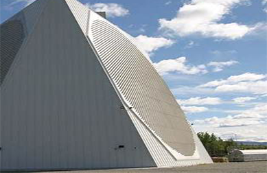
- Satcom & ground: waveguide preferred; a microwave isolator is often specified in high-power links; consider vacuum cooling, radiation, thermal cycling; evaluate power‑thermal‑frequency coupling.
- MRI: a circulator separates Tx/Rx coils; assess strong‑field effects and RF heating vs SAR/stability.
FAQ
Q1: How to use an RF isolator (microwave isolator class) safely?
Keep SWR low, respect power/thermal limits, and validate IL/Isolation over temperature. Place the device to protect the PA from reflected power.
Q2: RF isolator vs RF circulator — what’s the difference?
An RF isolator is a two‑port protector that passes forward and absorbs reverse; an RF circulator is a three‑port router with one‑way flow (1→2→3→1).
Q3: Do I always need waveguide for high power?
Not always, but waveguide excels for very high power/low loss/thermal robustness. Coax can work with careful derating and cooling.
References
- Pozar, Microwave Engineering, Wiley.
- Collin, Foundations for Microwave Engineering, McGraw‑Hill.
- IEEE T‑MTT articles on ferrite circulators/isolators.
- NRL/NASA tech reports on radar/satcom ferrite components.
Relateds


About the Author

HzBeat Editorial Content Team
Marketing Director, Chengdu Hertz Electronic Technology Co., Ltd. (Hzbeat)
Keith has over 18 years in the RF components industry, focusing on the intersection of technology, healthcare applications, and global market trends.