Microstrip vs. Drop‑In Circulators: Principles, Design Structures, and Advanced Applications
Updated on:
Keywords: microstrip circulator,drop-in circulator,ferrite circulator,Insertion Loss,Isolation
This journal‑style article compares microstrip circulators and drop-in circulators in depth. We start from first‑principle physics (gyromagnetism and the Polder tensor), proceed through junction structures and performance metrics, then detail integration methods and advanced applications from L‑ to W‑band. A technical FAQ and references are included for further study.
Explore Related HzBeat Products:
Microstrip Circulators · Drop‑In Circulators · Contact Technical Support
1) Introduction
Circulators are three‑port passive components enabling directional energy routing—classically 1→2→3—while presenting high attenuation in the reverse directions. They protect power amplifiers (PAs) from load mismatch, stabilize oscillation conditions, and enable duplex operation in transceiver chains. While waveguide and coaxial forms remain important, modern RF front‑ends rely increasingly on two families: microstrip circulators, which are planar and co‑designed with the PCB; and drop‑in circulators, which are housed and factory‑tuned for modular assembly.
This article delivers a detailed comparison for engineers who must reconcile electrical performance with mechanical, thermal, and manufacturability constraints. We begin by establishing the physical origin of non‑reciprocity in ferrites, then examine design structures for microstrip and drop‑in types, quantify performance trade‑offs, and finish with integration guidelines and application‑specific recommendations across bands. A technical FAQ precedes the references to address recurring design questions.
2) Ferrite Physics and Non‑Reciprocity
2.1 Larmor Precession and the Polder Tensor
Ferrimagnetic materials under a static magnetic field B0 exhibit gyromagnetic behavior wherein magnetic dipole moments precess about the bias direction with the Larmor frequency. The macroscopic effect is an anisotropic permeability described by the Polder tensor. For small‑signal operation near but below ferromagnetic resonance (FMR), the relative permeability tensor contains off‑diagonal terms ±jκ that couple orthogonal field components with a sense of rotation. As a consequence, left‑hand and right‑hand circularly polarized field components propagate with different phase constants—a necessary condition for non‑reciprocity and the foundation of circulator action.
2.2 Junction Energy Flow and Bias Orientation
The three‑port Y‑junction can be visualized as three transmission‑line arms meeting over a ferrite disc. With the bias normal to the plane, modal field rotation interacts with the ferrite’s gyromagnetic properties to favor a clockwise (or counterclockwise) energy flow depending on the bias polarity. Reversing the bias reverses the circulation sense. Finite element field plots (from full‑wave solvers) show the modal splitting around the junction and highlight sensitivity to ferrite diameter, thickness, and the proximity of metal boundaries.
2.3 Bandwidth, Power, and Linearity
Bandwidth arises from the combined frequency response of the ferrite dispersion and the matching networks used at each port. A broader ferrite linewidth can widen usable bandwidth but may raise insertion loss. Linearity is generally excellent as circulators are passive; yet at high average or peak power, magnetization dynamics approach non‑linear regimes, manifesting as isolation droop or compression. Thermal management is essential: the ferrite’s saturation magnetization Ms decreases with temperature, shifting the operating point unless compensated.
3) Microstrip Circulators—Design Structures
3.1 Planar Y‑Junction on Ferrite or Composite Substrates
Microstrip circulators implement the junction as printed conductors on ferrite or a bonded dielectric‑ferrite stack. Each arm is typically 50 Ω, with a matching cell at each port to flatten return loss across the band. Design proceeds via EM simulation that accounts for the open microstrip fields, substrate anisotropy, via fences, and the metal lid or shield. Because the structure is planar, it can be embedded adjacent to active stages to minimize interconnect length, thereby lowering insertion loss and improving noise performance in receiver paths.
3.2 Stack‑Up, Grounding, and Shielding
Stack‑up control is crucial: dielectric constant, thickness, copper roughness, and ground spacing set the characteristic impedance and modal confinement. Via fences around the junction reduce radiation and suppress unintended cavity modes. A thin metal lid provides EMI containment while maintaining a low Z‑height. Designers must avoid creating resonant cavities between the lid and the PCB; lossy absorbers or carefully placed standoffs help damp spurious resonances without excessively loading the junction.
3.3 Bias Magnet Implementation
Permanent magnets (e.g., SmCo or NdFeB) above or below the ferrite establish the DC bias. Uniformity matters: field gradients or edge demagnetization degrade isolation. In compact modules, shims and pole‑piece geometry even out the field. Where thermal drift is a concern, temperature‑stable grades or compensation strategies maintain Ms within design range.
3.4 Matching Networks and Bandwidth Enhancement
Simple quarter‑wave or lumped matching networks at each port equalize return loss and broaden bandwidth. At higher GHz, distributed stubs integrated into the microstrip reduce parasitics relative to discrete components. Some designs employ multi‑section matching with moderate Q to trade a flat passband for slightly higher insertion loss.
3.5 Variants: Embedded, SMT, and LTCC‑Like Planar Implementations
Beyond classic microstrip, embedded stripline‑like forms reduce radiation by enclosing the fields. SMT microstrip circulators adopt bent pins or tabs to simplify board assembly. LTCC‑style multilayer implementations embed conductors and magnetic layers in ceramic, shrinking area and enhancing shielding at the expense of fabrication complexity.
3.6 Strengths and Challenges
- Strengths: Minimal interconnect loss, lowest Z‑height, excellent co‑design with PAs/LNAs, suitability for dense phased‑array tiles.
- Challenges: Sensitivity to stack‑up and assembly tolerances; open‑structure radiation; limited reworkability once soldered.
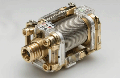
4) Drop‑In Circulators—Design Structures
4.1 Housed Ferrite Junctions with Defined Interfaces
Drop‑in circulators encapsulate the ferrite junction in a machined metal housing with precisely controlled cavity geometries. Ports are realized as solder tabs, pins into stripline, or coaxial connectors (SMA/SMP, N‑type). The manufacturer tunes the junction via adjusters (e.g., screws, dielectric shims) to center frequency and flatten response, then validates S‑parameters across temperature.
4.2 Mechanical and Thermal Architecture
Metal housings provide robust shielding and a direct thermal path to the baseplate. Flatness, torque specification, and thermal interface material (TIM) selection determine long‑term stability under power cycling. Mechanical design must withstand vibration and shock for aerospace or defense uses. The added height relative to microstrip is offset by superior heat spreading and serviceability.
4.3 Structural Variants
- Tab‑Style Drop‑Ins: Solder‑in tabs transition to planar lines; compact footprint for modules.
- Connectorized Modules: SMA/SMP for bench and rack; fast lab swaps and measurement.
- Waveguide Drop‑Ins: For mm‑wave and high‑power links where waveguide loss is attractive and power density is high.
4.4 Strengths and Challenges
- Strengths: Factory‑tuned repeatability, rugged mechanics, superior thermal handling, and straightforward field replacement.
- Challenges: Greater Z‑height and footprint; additional transitions that may add small insertion loss; less freedom to co‑shape the RF neighborhood.

Figure 3 — Modular assembly context typical for drop‑in parts (Unsplash, CC0).
5) Performance Metrics and Deep Comparison
5.1 Parameter Definitions
- Insertion Loss (IL): Power dissipated or reflected in the intended path; influenced by conductor/dielectric loss, mismatch, and junction dissipation.
- Isolation: Reverse‑path attenuation; depends on ferrite bias uniformity, junction symmetry, and matching quality.
- Return Loss / VSWR: Port match quality; poor match raises overall system ripple and coupling to adjacent networks.
- Bandwidth: Frequency span where IL, isolation, and return loss meet the spec simultaneously.
- Power Handling: CW and peak; limited by ferrite saturation and thermal path; duty cycle critical.
- Temperature Stability: Spec drift vs. temperature due to Ms variation and mechanical changes.
5.2 Typical Ranges by Band (Indicative)
| Band | Microstrip IL | Drop‑In IL | Isolation | VSWR | Notes |
|---|---|---|---|---|---|
| L/S (1–4 GHz) | 0.3–0.6 dB | 0.3–0.5 dB | ≥ 20–25 dB | ≤ 1.25–1.35 | Microstrip compact; drop‑in robust for PA protection. |
| C/X (4–12 GHz) | 0.35–0.7 dB | 0.35–0.6 dB | ≥ 18–25 dB | ≤ 1.25–1.35 | AESA tiles favor planar; benches prefer connectorized. |
| Ku/Ka (12–40 GHz) | 0.4–0.8 dB | 0.4–0.7 dB | ≥ 18–24 dB | ≤ 1.3–1.5 | Tight tolerance; thermal control increasingly critical. |
| V/W (50–110 GHz) | 0.6–1.2 dB | 0.6–1.0 dB | ≥ 15–22 dB | ≤ 1.4–1.6 | Waveguide hybrids and LTCC/ceramic options appear. |
These values are indicative and depend on ferrite grade, bias configuration, matching, and mechanical design. Always consult the device datasheet and validate in‑system with calibrated fixtures.
5.3 Trade‑Off Narratives
Microstrip excels where interconnect length must be minimized and Z‑height is constrained. Its IL advantage stems from avoiding extra connectors, but it demands strict stack‑up and shielding discipline. Drop‑ins shine where mechanical robustness, thermal routing, and serviceability dominate; their IL is competitive, and their isolation consistency is often superior across hosts due to factory tuning and enclosure control.
6) Integration & Manufacturing Considerations
6.1 Planar (Microstrip) Integration
- Stack‑Up Control: Lock dielectric materials and thickness early; specify copper roughness and plating to stabilize loss.
- Shielding: Use via fences and metal lids; avoid creating parallel‑plate resonators; consider absorbers if needed.
- Bias Field: Verify uniformity with magnetostatic simulation; include shims; check demagnetization margins near edges.
- Thermal Path: Add copper pours/thermal vias under ferrite; consider heat‑spreaders to the chassis.
- Test Strategy: Design calibration standards near the junction; de‑embed launches to measure true IL and isolation.
6.2 Modular (Drop‑In) Integration
- Mounting: Ensure baseplate flatness and torque; select TIM to minimize contact resistance without pumping‑out under cycling.
- Transitions: Keep planar transitions short and broadband; simulate launch structures to avoid resonances.
- Reliability: Validate under vibration and temperature cycling; monitor isolation drift with logging fixtures.
- Maintainability: Provide access for replacements; standardize connector types to simplify spares.
7) Applications from L‑ to W‑Band
7.1 5G/6G Radio Units and Small Cells
Planar microstrip circulators are compelling for outdoor radios and small cells where space and weight are constrained. Embedding the device near PAs reduces loss and improves efficiency. At sub‑6 GHz, careful shielding tames radiation; at FR2/mmWave, LTCC‑like approaches become attractive for repeatability.
7.2 AESA Radar Tiles
Phased‑array tiles demand dense integration and consistent phase behavior across elements. Microstrip circulators co‑packaged with PAs/LNAs allow short interconnects, minimizing uncertainty in amplitude/phase. For high‑power backplane modules or field‑replaceable assemblies, drop‑ins enable service without reworking the board.
7.3 SATCOM Terminals and Gateways
User terminals benefit from planar solutions for low profile and cost, while hub or gateway stations may favor drop‑ins or waveguide drop‑ins for power handling and thermal headroom. At Ka‑band, connector choice and launch design dominate the loss budget.
7.4 Test & Measurement and Amplifier Protection
Connectorized drop‑ins are ideal in labs and production lines for their swap‑ability and known calibration. Embedded microstrip versions appear on evaluation boards to protect devices under test and to demonstrate system‑level performance in application notes.
8) Emerging Trends: LTCC, Magnetless, and IC Paths
8.1 LTCC and Multilayer Integration
LTCC enables multilayer routing, embedded passive matching, and improved shielding for circulators. By confining fields within ceramics, designers reduce parasitics and radiation while tightening tolerances. The cost and process complexity are higher, but mmWave repeatability often justifies the trade.
8.2 Magnetless Non‑Reciprocity (Research)
Spatiotemporal modulation in CMOS or III‑V ICs emulates non‑reciprocity by periodically varying reactive elements, breaking time‑reversal symmetry without ferrites. These magnetless circulators are attractive for on‑chip integration and beamforming networks; however, noise figure, linearity under power, and spectral purity remain active research challenges compared to ferrite devices.
8.3 Thermal‑Mechanical Co‑Design and Reliability
Next‑generation modules incorporate copper coins, vapor chambers, and low‑profile absorbers to manage heat and EMI simultaneously. Mechanical damping strategies address vibration; conformal coatings improve moisture robustness. For drop‑ins, baseplate standards and TIM selection are being harmonized across vendors to simplify replacement logistics.
9) Technical FAQ
Q1. What primarily sets the isolation of a microstrip circulator?
Ferrite saturation magnetization and bias uniformity dominate, followed by junction symmetry and matching network balance. Uneven bias or dimensional skew reduces modal splitting and isolation. Use magnet shims, precise ferrite polishing, and symmetric matching.
Q2. How does temperature influence performance?
Rising temperature lowers Ms, shifting the operating point and narrowing the isolation plateau. Employ temperature‑stable ferrites, thermal path optimization, and, where possible, compensation magnets to limit drift.
Q3. Can a drop‑in circulator be re‑biased to another band?
Only within a narrow margin. Housing, ferrite geometry, and matching networks fix the band. Significant retuning requires redesign or a different model.
Q4. Why do insertion losses differ between microstrip and drop‑in?
Microstrip avoids connector transitions but adds conductor/dielectric loss in open planar fields. Drop‑ins have short internal paths and metal enclosures but add transition/connector loss. Both benefit from precise matching and surface finish control.
Q5. Which type should I pick for high‑power mmWave links?
Consider waveguide or rugged drop‑in modules with excellent thermal paths if power density is high. For compact phased‑array tiles, planar or LTCC implementations may be preferable to meet height and routing constraints.
References
- LibreTexts — Ferrite Components: Circulators and Isolators (background theory).
- Wikipedia — Circulator (overview of types and principles).
- Smiths Interconnect Blog — Anatomy of a Microstrip Isolator and Circulator.
- Smiths Interconnect — Product overview for coaxial/microstrip/drop‑in circulators.
Relateds

About the Author

HzBeat Editorial Content Team
Sara is a Brand Specialist at Hzbeat, focusing on RF & microwave industry communications. She transforms complex technologies into accessible insights, helping global readers understand the value of circulators, isolators, and other key components.