What Is an RF Circulator and How Does It Work? | HzBeat Knowledge Center
Updated on:
Keywords: RF circulator, isolator, ferrite circulator, non-reciprocal device, waveguide circulator, coaxial circulator, microstrip circulator, SMT circulator, S-parameters, insertion loss, isolation, VSWR, power handling, VNA calibration
Introduction
An RF circulator is a three-port, non-reciprocal passive device that routes energy directionally in the order 1→2→3→1. In transmit/receive front ends, this “one-way valve” enables duplexing and protects power amplifiers (PAs) and low-noise amplifiers (LNAs) from reflections. A two-port isolator is simply a circulator with the third port terminated in a matched load. This article explains how the ferrite-bias mechanism works, how to read the key specs, which form factors to pick (waveguide, coaxial, microstrip/SMT), and how to verify performance on a vector network analyzer (VNA).

Circulator in 90 seconds: behavior & S-parameters
Ideally, a 3-port circulator passes forward paths near-losslessly—S21≈0 dB, S32≈0 dB, S13≈0 dB—while strongly rejecting the reverse paths (S12, S23, S31 ≪ 0 dB). Real devices trade insertion loss (IL), isolation (ISO), and return loss (RL)/VSWR across the operating band and temperature. Converting a circulator into an RF isolator is as simple as placing a matched 50 Ω termination on the dump port to absorb reflections.
Tips:
For PA protection, route PA → Port‑1, antenna → Port‑2, and terminate Port‑3 with 50 Ω. Reflected power is safely dissipated in the load.
Why it works—ferrite non-reciprocity, the short physics
Under a static magnetic bias, gyromagnetic ferrites exhibit a tensor permeability that makes the RF field precess. This breaks time‑reversal symmetry and introduces a preferred rotation—hence the name “circulator.” In a resonant Y‑junction or a loaded transmission‑line junction, careful choice of ferrite saturation magnetization (4πMs), bias field H, and geometry sets the center frequency and bandwidth. Higher 4πMs supports higher frequencies; dielectric loading can miniaturize the junction at the cost of Q and potentially higher IL.
Spec deep-dive: how to read, target, and negotiate
Insertion Loss (IL)
IL directly reduces EIRP in TX and raises noise figure in RX. For premium RF circulator designs, 0.2–0.5 dB is common in narrow to moderate bands; ultra‑wideband units may be 0.6–0.9 dB+.
- Design knobs: ferrite Q, conductor finish, dielectric tanδ, junction phasing.
- System view: every 0.5 dB costs ~12% TX power at the antenna.
Isolation (ISO)
ISO protects PAs/LNAs from reflected energy and crosstalk. Typical targets: ≥ 20–30 dB (waveguide often higher). Broadening bandwidth usually lowers peak ISO.
- Watch‑outs: magnet/bias drift with temperature, assembly tolerances, housing stress.
- Spec tactic: negotiate ISO at band edges separately from center‑band.
Return Loss / VSWR
Good RL (≥ 14–18 dB) reduces mismatch ripple and hotspots. Specify RL at all three ports; poor match on the dump port degrades effective isolation.
Power Handling
SMT/microstrip devices handle watts to tens of watts; coaxial/drop‑in tens to hundreds; waveguide can be kW‑class. Consider VSWR‑withstand under fault (open/short) and pulse heating.
Bandwidth & Flatness
Bandwidth ranges from ~5–10% (narrow) to 30%+ (wide). Clarify in‑band IL ripple and ISO flatness—these are more meaningful than headline “min/max”.
Temperature & Stability
Bias field and 4πMs drift shift the junction, moving IL/ISO peaks. Ask for derating curves and Δf vs. °C data.
Form factors & when to choose them
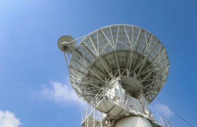
Waveguide Circulator
Low IL, high ISO, and superb thermal paths—ideal for radar and SatCom HPAs. Use standard WR flanges; ensure surface flatness and torque spec to maintain RL. Downside: size/mass.
Coaxial Circulator
Flexible 50 Ω interconnect (SMA/N/K/7‑16). Great for test benches, base stations, and modular radios. Watch connector repeatability and torque.
Drop‑in / Microstrip
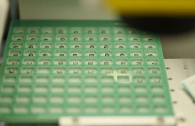
Compact, cost‑effective, PCB‑integrated. Requires controlled stack‑up, via fences, cavity control, and magnetic keep‑out. Copper roughness and dielectric loss directly impact IL.
SMT Circulator
Solder‑reflow capable, ultra‑miniaturized. Verify land pattern, thermal pad, reflow profile, and magnetic interactions with nearby sensors. Usually lower power.

Integration notes—make it work on your board or rack
- Mechanical: For drop‑ins, keep cavity planarity; avoid ferromagnetic screws near the junction. For waveguide, respect flange flatness, surface finish, and gasket compression.
- Thermal: Provide a low‑θ path (copper coin, metal base, heat spreader). Model worst‑case with reflected‑power heating when VSWR spikes.
- EMC & Bias Leakage: Magnets can disturb compasses/Hall sensors. Use shields or distance; check for coupling into LNAs/VCOs.
- Magnetic Safety: Define keep‑out for SSDs/sensors; mark polarity to aid serviceability.
- Reliability: Shock/vibration can detune bias. For defense/space, consider magnet grade, adhesive selection, bake‑out, and outgassing limits.
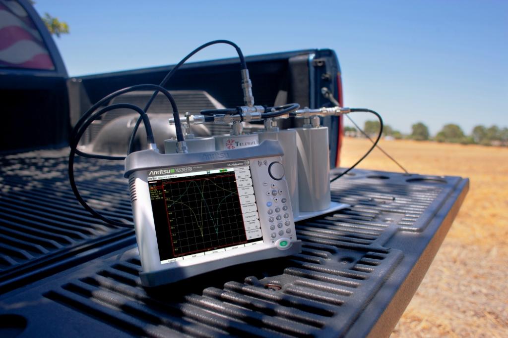
VNA test & calibration—separating DUT from setup
Many “bad parts” are calibration issues. Calibrate at the device plane (SOLT/TRL) and de‑embed fixtures. Verify with port‑by‑port RL, IL on forward path, and ISO on reverse paths. For coaxial devices use torque wrenches; for waveguide, measure RL before/after flange reassembly. For SMT/drop‑in, use probe or well‑characterized fixtures and compensate cable‑movement drift.
- Checks: repeatability over re‑connects; temperature sweeps; power‑sweep IL/ISO; ripple vs. fixture resonances.
- Documentation: save Touchstone (S3P) and annotate calibration kits, cables, and dates. It saves days in failure analysis.
Where circulators shine—use-case patterns
- TX/RX duplexing: Passive separation in high‑power chains without lossy active T/R switches at microwave power levels.
- PA protection: With the dump port terminated, the isolator safely absorbs reverse power and protects the PA.
- Oscillation control: Breaking unintended feedback in narrowband high‑gain amplifiers and oscillation‑prone test setups.
- Production test: Stabilize source‑to‑DUT; protect signal sources during power sweeps; reduce standing‑wave ripple.
- Industrial sensing/heating: Variable‑load environments benefit from one‑way energy flow.
Selection & procurement checklist
- Band & bandwidth: L/S/C/X/Ku/Ka; fractional BW. Specify in‑band IL ripple and ISO floor.
- IL/ISO/RL vs. temperature: Request curves and corner conditions; capture Δf vs. °C.
- Power & VSWR withstand: Average/peak, fault cases (open/short), duty cycle, pulse width.
- Form factor: WR‑xx flange, SMA/N/K/7‑16, drop‑in pad map, SMT land pattern; magnet keep‑out.
- Reliability & screening: Shock/vibe, humidity, thermal cycling, magnet aging; for space, outgassing/ECSS.
- Compliance: RoHS/REACH; material declarations; magnet safety for shipping.
- Data package: S3P files, outline drawing, mounting torque, reflow profile (SMT), antenna VSWR assumptions.
FAQs
Q1. Is an isolator just a circulator with a load?
Yes. Terminate the third port with a 50 Ω matched load and you get a two‑port isolator that absorbs reverse power.
Q2. Why do ISO and IL drift with temperature?
Bias field and ferrite parameters (H, 4πMs) change with temperature, shifting junction phase. Good magnets, thermal design, and margin mitigate this.
Q3. Can circulators work at mmWave?
Yes—junction waveguide and thin‑film ferrite approaches extend to Ka‑band and beyond, though loss and bandwidth targets become more challenging.
Q4. What is a “good” IL?
Application‑dependent. ≤ 0.3 dB is excellent for high‑end microwave; 0.3–0.6 dB is common in compact designs; ultra‑wideband units may be higher.
Relateds


About the Author

HzBeat Editorial Content Team
Sara is a Brand Specialist at Hzbeat, focusing on RF & microwave industry communications. She transforms complex technologies into accessible insights, helping global readers understand the value of circulators, isolators, and other key components.