RF Isolator & Circulator Installation Guide: Direction, Matching, Heat Dissipation, and Testing
Updated on:
Keywords: RF isolator installation, RF circulator installation, microstrip circulator layout, drop-in isolator mounting, coaxial circulator, waveguide circulator, RF heat dissipation, S-parameter testing
This guide focuses purely on how to install RF isolators and circulators in real systems: how to confirm direction, how to mount each package type, how to build a good thermal path, and how to test the assembly after installation.
No theory, no long introductions—only practical, repeatable steps that RF and microwave engineers can apply on the bench and in production.
1. Direction and Port Orientation
Before tightening a single screw or touching a soldering iron, confirm one thing first: which way the power is supposed to flow.
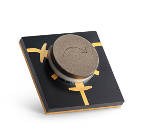
1.1 Reading arrows, port numbers, and labels
On most commercial isolators and circulators you will find:
- Arrows printed on the housing (for example, “1 → 2”).
- Port numbers engraved or screen-printed near pins/connectors (P1, P2, P3).
- Simple labels such as “IN / OUT / LOAD”.
Align these markings with your schematic and PCB silkscreen before installation. A few seconds of checking here can prevent hours of debugging later.
1.2 Practical port assignments for circulators
When using a circulator as a protector in a transmit chain, the most common wiring is:
- Port 1: power amplifier output.
- Port 2: antenna or system output.
- Port 3: external 50 Ω load (absorbs reflected power).
Mark this clearly on your mechanical drawing or PCB silkscreen so the assembly team cannot “invent” their own orientation.
1.3 Are installation rules the same for isolators and circulators?
Mechanically they follow the same rules—flat mounting, correct torque, good ground and thermal contact. The main installation difference is:
- Isolators are two-port; you only connect input and output.
- Circulators are three-port; the “third” port must be treated properly (typically connected to a 50 Ω load in PA protection use cases).
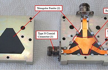
2. Mechanical Installation by Package Type
Isolators and circulators are available as microstrip/SMT, drop-in, coaxial and waveguide versions. The goal is always the same: solid mechanical support, reliable RF connection and an efficient thermal path.
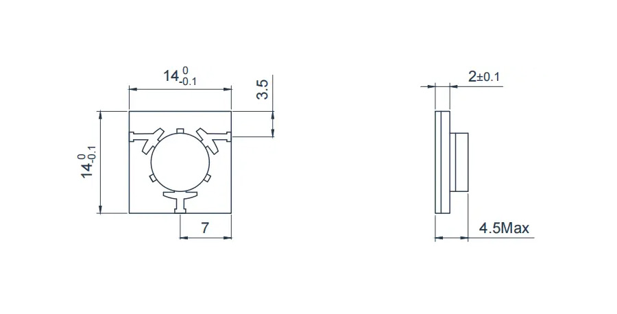
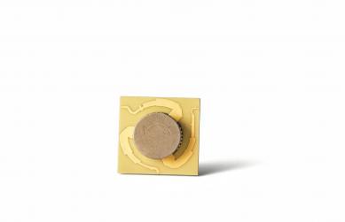
2.1 Microstrip / SMT devices
Microstrip and SMT devices sit directly on the PCB. Typical examples include microstrip circulators and microstrip isolators.
- Prepare the PCB land pattern. Follow the recommended pad and via layout from the datasheet:
- 50 Ω line width for the chosen substrate.
- Ground via “fences” around RF traces and under the device.
- Enough copper for heat spreading beneath the body.
- Check orientation before soldering. Make sure the port numbering/arrow on the device matches the PCB orientation and your system signal flow.
- Run the solder process. Use the recommended reflow or hand-solder profile:
- Avoid tilting or rocking the part while the solder is molten.
- Inspect for lifted corners or incomplete wetting on ground pads.
- Inspect and, if needed, rework. Clean flux residues and correct any misalignments before moving to RF testing.
2.2 Drop-in isolators and circulators
Drop-in packages are common in radar and high-power communication modules. The device sits in a machined cavity, with RF pins soldered to the PCB and the base bolted to a heatsink or chassis. See HzBeat’s drop-in isolators and drop-in circulators as typical implementations.
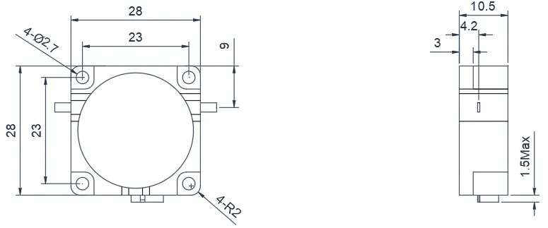
- Prepare the cavity and PCB cutout.
- Machine the pocket so the base sits flat with no rocking.
- Route PCB traces so the RF pins land with minimal lead length.
- Check clearance for screw heads, tools and any nearby components.
- Apply thermal interface material if needed.
- Use a thin, even layer of grease or a compliant thermal pad.
- Keep material away from RF pads and solder areas.
- Place the device and tighten screws.
- Align RF pins with PCB pads before tightening.
- Tighten screws in a cross pattern, gradually increasing torque.
- Solder RF pins.
- Use only as much solder as needed for reliable joints.
- Avoid heating the housing excessively during rework.
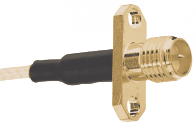
2.3 Coaxial devices
Coaxial isolators and circulators are installed via SMA, N-type, or similar RF connectors.
- Use a dedicated torque wrench for the connector type.
- Support the device mechanically with brackets or mounting plates so the connectors do not carry bending loads.
- For higher power, mount the housing to a heatsink or metal panel with thermal interface material.
2.4 Waveguide devices
Waveguide versions bolt directly between flanges in the waveguide run.
- Clean flange faces; remove dust, burrs and old gasket residue.
- Install the correct gasket or choke interface for the band.
- Tighten flange screws evenly around the pattern.
- Support long sections of waveguide so the device is not acting as a mechanical beam.
3. RF Matching and PCB/Layout Considerations
A mechanically perfect installation can still fail if the RF environment around the device is poorly matched. Layout and grounding are part of the installation work.
3.1 Transmission line design
- Use 50 Ω microstrip or stripline traces as required for your substrate.
- Keep connections between the device and the rest of the RF chain short and direct.
- Use gentle bends (45° or mitered) instead of sharp 90° corners at high frequencies.
3.2 Grounding and via fences
- Place dense via fences along RF traces and beneath the device’s ground pads.
- Connect the device ground to a solid reference plane and, where needed, to the metal chassis.
- Keep noisy digital or switching lines away from the device area to avoid coupling.
3.3 Treating the third port of a circulator
When using a circulator as an isolator:
- Connect the “dump” port to a high-quality 50 Ω load with sufficient power rating.
- Mount the load on a heatsink or chassis panel—this port sees reflected power.
- During testing, confirm that reverse power from the antenna side ends up at the load and not back at the PA.
4. Heat Dissipation and Power Handling
Installation is not complete until the thermal path is defined. Devices that run within their temperature limits are far more stable and reliable over time.
4.1 Check the relevant power ratings
- CW power: continuous power level allowed at a given ambient or baseplate temperature.
- Peak power: allowed pulse power level with a given duty cycle.
- Reverse power: how much reflected power can be safely dissipated.
Plan your installation so that worst-case VSWR events do not push the device beyond these ratings.
4.2 Build a solid thermal path
- Use flat, well-machined mounting surfaces.
- Add a thin thermal pad or grease between the base and the heatsink when needed.
- Orient heatsinks along the airflow direction inside the enclosure.
- On PCBs, use thermal vias under the device to spread heat into inner copper planes and any attached metal carrier.
4.3 Validate temperature in early builds
- Measure case temperature with a thermocouple or IR camera during power tests.
- Test with realistic worst-case mismatches (for example, open, short or specified VSWR at the antenna port).
- If temperatures are too high, upgrade the heatsink, improve airflow or limit the allowable power level.
5. Testing After Installation
A good installation is always followed by measurement. Testing confirms that mounting, soldering and thermal design have not degraded performance.
5.1 Vector network analyzer (VNA) checks
- Calibrate. Run a proper 2-port or 3-port calibration across the operating band.
- Measure key S-parameters.
- For isolators: S21 (forward insertion loss), S11/S22 (return loss at each port).
- For circulators: forward paths (for example S21, S32, S13) and reverse isolation terms.
- Compare with specification. Check that measured values meet or exceed datasheet targets.
5.2 Power testing
After S-parameter verification, confirm behavior at real RF power:
- Use a PA, directional coupler and power meter or power analyzer.
- Observe forward and reflected power under normal and fault conditions.
- Monitor device case temperature over time during high-power operation.
5.3 System-level functional tests
- Confirm that the PA does not oscillate or shut down unexpectedly with the device installed.
- Verify that receiver performance meets requirements with all RF paths in place.
- If available, log VSWR, current and temperature telemetries for longer-term runs.
6. Quick Installation Checklist
- ✅ Direction confirmed (arrow and port numbers match system power flow).
- ✅ Correct port usage for circulators (third port terminated or routed as designed).
- ✅ Mounting surfaces flat and clean; screws tightened evenly to reasonable torque.
- ✅ PCB pads and vias follow manufacturer land pattern and 50 Ω design.
- ✅ Thermal path in place (heatsink, spreader, thermal interface as required).
- ✅ External loads fitted and properly rated for circulator dump ports.
- ✅ S-parameters measured and within specification.
- ✅ Power and temperature tests performed under worst-case mismatch.
7. FAQ: Common Installation Questions
Mechanically they are almost identical: both need flat mounting, good contact, proper torque and reliable thermal paths. The main difference is on the wiring side—the third port of a circulator must be handled correctly (often with a 50 Ω load), whereas an isolator has only two ports to connect.
Align the arrow with the intended forward power direction. In a typical transmit chain that means: PA → isolator → antenna or system output. Always double-check this against your schematic and layout before installation.
An unterminated third port can cause unstable VSWR and unpredictable behavior. If that port is supposed to absorb reflected power, it should be connected to a suitable 50 Ω termination with enough power and thermal margin.
It is better to use bare or lightly treated metal where the device base contacts the surface. Thick coatings increase thermal resistance and may compromise grounding. If coating is unavoidable, verify device temperature carefully during power tests.
For new designs, prototypes and high-reliability systems, VNA checks are strongly recommended. For mature, stable production lines you may rely on incoming inspection plus periodic sampling, but initial qualification should always include S-parameter verification.
From an installation point of view:
- Microstrip/SMT: best for compact, highly integrated PCB designs.
- Drop-in: suited for high-power modules with solid metal carriers and clear cavities.
- Coaxial: ideal for setups built around RF cabling, test racks or flexible lab configurations.
- Waveguide: used when you already work in waveguide for that band and power level.
Need Help With a Specific Design?
If you are integrating RF isolators or circulators into a radar, SatCom, medical imaging or 5G/6G platform and want installation advice on direction, mechanical layout or thermal paths, you can reach the HzBeat team at [email protected] or via the contact page: https://www.hzbeat.com/contact.html.
Relateds

About the Author

HzBeat Editorial Content Team
Marketing Director, Chengdu Hertz Electronic Technology Co., Ltd. (Hzbeat)
Keith has over 18 years in the RF components industry, focusing on the intersection of technology, healthcare applications, and global market trends.